- 您现在的位置:买卖IC网 > Sheet目录3862 > PIC18F45J11-I/ML (Microchip Technology)IC PIC MCU FLASH 32K 2V 44-QFN
dsPIC30F3014/4013
DS70138G-page 150
2010 Microchip Technology Inc.
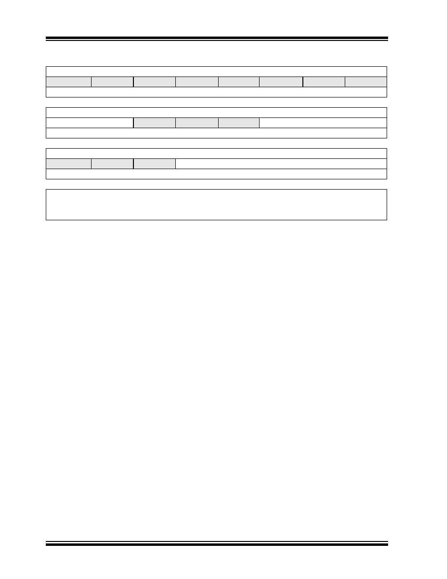
REGISTER 20-3:
FOSC: OSCILLATOR CONFIGURATION REGISTER
UU
U
—
bit 23
bit 16
R/P
U
R/P
FCKSM<1:0>
—
—FOS<2:0>
bit 15
bit 8
U
R/P
—
—FPR<4:0>
bit 7
bit 0
Legend:
R = Readable bit
W = Writable bit
U = Unimplemented bit, read as ‘0’
-n = Value at POR
‘1’ = Bit is set
‘0’ = Bit is cleared
x = Bit is unknown
bit 23-16
Unimplemented: Read as ‘0’
bit 15-14
FCKSM<1:0>: Clock Switching and Monitor Selection Configuration bits
1x
= Clock switching is disabled, Fail-Safe Clock Monitor is disabled
01
= Clock switching is enabled, Fail-Safe Clock Monitor is disabled
00
= Clock switching is enabled, Fail-Safe Clock Monitor is enabled
bit 13-11
Unimplemented: Read as ‘0’
bit 10-8
FOS<2:0>: Oscillator Group Selection on POR bits
111
= PLL oscillator; PLL source selected by FPR<4:0> bits (see Table 20-2)
011
= EXT: External Oscillator; OSC1/OSC2 pins; external oscillator configuration selected by
FPR<4:0> bits
010
= LPRC: Internal Low-Power RC
001
= FRC: Internal Fast RC
000
= LPOSC: Low-Power Crystal Oscillator; SOSCI/SOSCO pins
bit 7-5
Unimplemented: Read as ‘0’
bit 4-0
FPR<4:0>: Oscillator Selection within Primary Group bits (see Table 20-2)
发布紧急采购,3分钟左右您将得到回复。
相关PDF资料
SFW15R-2STE1
SFW15R-2STE1-FFC/FPC CONN
PIC18F26J11-I/ML
IC PIC MCU FLASH 64K 2V 28-QFN
PIC18F46K20-E/ML
IC PIC MCU FLASH 32KX16 44QFN
PIC24FJ64GA002-I/SO
IC PIC MCU FLASH 64KB 28SOIC
PIC16C711-04/P
IC MCU OTP 1KX14 A/D 18DIP
PIC18LF26K22-I/SP
IC PIC MCU 64KB FLASH 28SPDIP
PIC18F25K80-I/SP
MCU PIC 32KB FLASH 28SDIP
DSPIC33FJ12MC201-I/SS
IC DSPIC MCU/DSP 12K 20SSOP
相关代理商/技术参数
PIC18F45J11-I/PT
功能描述:8位微控制器 -MCU 32KB Flash 4KBRAM 12MIPS nanoWatt RoHS:否 制造商:Silicon Labs 核心:8051 处理器系列:C8051F39x 数据总线宽度:8 bit 最大时钟频率:50 MHz 程序存储器大小:16 KB 数据 RAM 大小:1 KB 片上 ADC:Yes 工作电源电压:1.8 V to 3.6 V 工作温度范围:- 40 C to + 105 C 封装 / 箱体:QFN-20 安装风格:SMD/SMT
PIC18F45J11T-I/ML
功能描述:8位微控制器 -MCU 32KB Flash 4KBRAM 12MIPS nanoWatt RoHS:否 制造商:Silicon Labs 核心:8051 处理器系列:C8051F39x 数据总线宽度:8 bit 最大时钟频率:50 MHz 程序存储器大小:16 KB 数据 RAM 大小:1 KB 片上 ADC:Yes 工作电源电压:1.8 V to 3.6 V 工作温度范围:- 40 C to + 105 C 封装 / 箱体:QFN-20 安装风格:SMD/SMT
PIC18F45J11T-I/PT
功能描述:8位微控制器 -MCU 32KB Flash 4KBRAM 12MIPS nanoWatt RoHS:否 制造商:Silicon Labs 核心:8051 处理器系列:C8051F39x 数据总线宽度:8 bit 最大时钟频率:50 MHz 程序存储器大小:16 KB 数据 RAM 大小:1 KB 片上 ADC:Yes 工作电源电压:1.8 V to 3.6 V 工作温度范围:- 40 C to + 105 C 封装 / 箱体:QFN-20 安装风格:SMD/SMT
PIC18F45J50-I/ML
功能描述:8位微控制器 -MCU Full Spd USB 32KB 4KBRAM nanoWatt RoHS:否 制造商:Silicon Labs 核心:8051 处理器系列:C8051F39x 数据总线宽度:8 bit 最大时钟频率:50 MHz 程序存储器大小:16 KB 数据 RAM 大小:1 KB 片上 ADC:Yes 工作电源电压:1.8 V to 3.6 V 工作温度范围:- 40 C to + 105 C 封装 / 箱体:QFN-20 安装风格:SMD/SMT
PIC18F45J50-I/PT
功能描述:8位微控制器 -MCU Full Spd USB 32KB 4KBRAM nanoWatt
RoHS:否 制造商:Silicon Labs 核心:8051 处理器系列:C8051F39x 数据总线宽度:8 bit 最大时钟频率:50 MHz 程序存储器大小:16 KB 数据 RAM 大小:1 KB 片上 ADC:Yes 工作电源电压:1.8 V to 3.6 V 工作温度范围:- 40 C to + 105 C 封装 / 箱体:QFN-20 安装风格:SMD/SMT
PIC18F45J50T-I/ML
功能描述:8位微控制器 -MCU Full Spd USB 32KB 4KBRAM nanoWatt RoHS:否 制造商:Silicon Labs 核心:8051 处理器系列:C8051F39x 数据总线宽度:8 bit 最大时钟频率:50 MHz 程序存储器大小:16 KB 数据 RAM 大小:1 KB 片上 ADC:Yes 工作电源电压:1.8 V to 3.6 V 工作温度范围:- 40 C to + 105 C 封装 / 箱体:QFN-20 安装风格:SMD/SMT
PIC18F45J50T-I/PT
功能描述:8位微控制器 -MCU Full Spd USB 32KB 4KBRAM nanoWatt RoHS:否 制造商:Silicon Labs 核心:8051 处理器系列:C8051F39x 数据总线宽度:8 bit 最大时钟频率:50 MHz 程序存储器大小:16 KB 数据 RAM 大小:1 KB 片上 ADC:Yes 工作电源电压:1.8 V to 3.6 V 工作温度范围:- 40 C to + 105 C 封装 / 箱体:QFN-20 安装风格:SMD/SMT
PIC18F45K20-E/ML
功能描述:8位微控制器 -MCU 32KB Flash 1536B RAM 25 I/O 8B RoHS:否 制造商:Silicon Labs 核心:8051 处理器系列:C8051F39x 数据总线宽度:8 bit 最大时钟频率:50 MHz 程序存储器大小:16 KB 数据 RAM 大小:1 KB 片上 ADC:Yes 工作电源电压:1.8 V to 3.6 V 工作温度范围:- 40 C to + 105 C 封装 / 箱体:QFN-20 安装风格:SMD/SMT